One interrupt to rule them all.
Overall Functionality
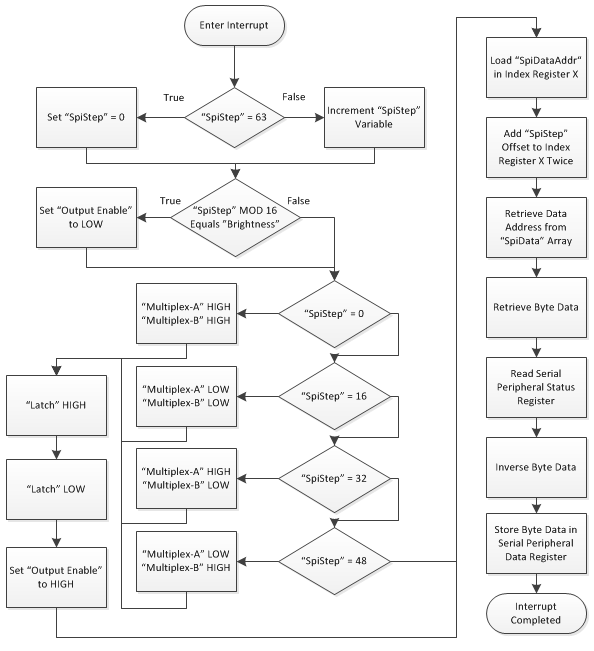
Below shows the general operation of the update cycle, it should be noted however that the interrupt is only executed after the sending of a byte over SPI.
Interrupt Sequence
The order in which the Serial Peripheral Interface (SPI) interrupt executes its subroutines is as follows:
- Increment SpiStep indexing variable
- Test for and handle Pulse Width Modulated (PWM) brightness control as necessary
- Test for and handle latching the shift registers as necessary
- Test for and handle changes to multiplexing and output control
- Read the SPI status from the SPI status register
- Locate and load the next byte to data into the SPI data register
SpiStep Incrementor
This variable is used to keep track of where the display is within its update sequence and will take one of 64 values (0 to 63). The SpiStep variable is used in each of the subsequent subroutines for testing or indexing and is usually left in both accumulators A and B to save repeatedly reloading the variable.
Brightness Control
PWM on the shift registers’ output enable pins is used to provide 15 linear steps of brightness. This is handled by firstly determining the value of SpiStep MOD 16 and then testing if that value matched the Brightness variable set by the brightness task, and if a match is found then the output enable line is driven low to disable the LEDs. The output enable line will automatically be pulled high again when the next sequence of data is latched onto the register outputs.
Latch Testing
As the SPI interrupt is run after data has been sent, the latch and multiplexing condition for the previous set of data is when SpiStep is at the beginning of the next sequence (0, 16, 32, 48). Once this condition has been detected then the appropriate subroutine must be executed to properly manipulate the multiplexing lines before latching the registers and enabling their outputs.
Multiplexing, Latching and Output Enabling
It had been chosen to use two of the pins on PortA of the micro controller as the multiplexing lines. As to not interfere with any other values on the port, bitwise and, exclusive or and or functions were used.
The shift registers are designed to be run at a very fast rate and even a momentary pulse on the latch line is able to latch the loaded data onto the register outputs. This means that the latch pin needed only to driven high and then immediately driven low.
After the correct rows have been selected by manipulating the multiplexing lines and the data has been transferred to the registers then the shift registers’ outputs can be enabled by driving their output enable line high.
Data Selection
After the aforementioned tasks have been completed then he next byte of data can be loaded into the SPI subsystem to be clocked into the shift registers. As the SPI interrupt has already been triggered, its flag must be cleared by reading the SPI status register (SPSR) and the writing new data to the SPI data register (SPDR). Reading the status register is easy and loading the next byte of data is somewhat simplified by the SpiData array and SpiStep variable, by using indirect addressing, starting at the beginning of the SpiData array (SpiDataAddr) and indexing by two times the SpiStep value (16 bit address values in SpiData) then the address of the intended data can be located. This data can then be easily loaded to an accumulator and stored to the SPI data register thus re-initiating the SPI subsystem to begin sending that data.
Interrupt Code
Below is the interrupt code implemented on the micro controller to handle this update process.
[code]
\ ( Latch and Multiplex ) ( When at 0,16,32,48 : Multiplex, then Latch, then Set Output Enable )
label Latch ( Pulse Register Latch ) PORTD LDAB %00100000 # ADDB PORTD STAB PORTD LDAB %00100000 # SUBB PORTD STAB ( /Pulse Register Latch ) ( Output On ) PortA LDAB 64 # ORAB PortA STAB ( /Output On ) RTS end-code
label 00-00 PORTA LDAB %00010000 # ORAB PORTA STAB Latch JSR RTS end-code
label 16-16 PORTA LDAB %11001111 # ANDB PORTA STAB Latch JSR RTS end-code
label 32-32 PORTA LDAB %00010000 # EORB PORTA STAB Latch JSR RTS end-code
label 48-48 PORTA LDAB %00110000 # EORB PORTA STAB Latch JSR RTS end-code
label TestLatch ( Assume SpiStep in A and B ) 0 # SUBB 0= IF 00-00 JSR ELSE TAB 16 # SUBB 0= IF 16-16 JSR ELSE TAB 32 # SUBB 0= IF 32-32 JSR ELSE TAB 48 # SUBB 0= IF 48-48 JSR ELSE THEN THEN THEN THEN TAB RTS end-code
label DoBrightness ( SpiStep Mod16 then test, Leave SpiStep in A and B ) 32 # SUBB 0< IF ( Lower Half ) TAB 16 # SUBB 0< IF ( Lower Quarter ) TAB ELSE TAB 16 # SUBB THEN ELSE TAB 48 # SUBB 0< IF TAB 32 # SUBB ELSE TAB 48 # SUBB THEN THEN ( End Offsets )
( Brightness Test ) Brightness SUBB 0= IF PortA LDAB 64 # EORB PortA STAB ELSE THEN TAB ( End Brightness Control ) RTS end-code
label DoSpiStep ( Increment SpiStep and leave in A and B ) SpiStep LDAA TAB 63 # SUBA 0= IF 0 # LDAB ELSE 1 # ADDB THEN SpiStep STAB TBA ( /Increment SpiStep ) RTS end-code
label DoData ( Assume SpiStep is in AB, Replace with Data ) SpiDataAddr LDX ABX ABX 0 ,X LDX 0 ,X LDAB RTS end-code
Label <SPI> DoSpiStep JSR DoBrightness JSR TestLatch JSR DoData JSR SPSR LDAA ( Read Status ) -1 # EORB SPDR STAB ( Write Inversed Data to Serial Data Register ) RTI end-code
[/code]
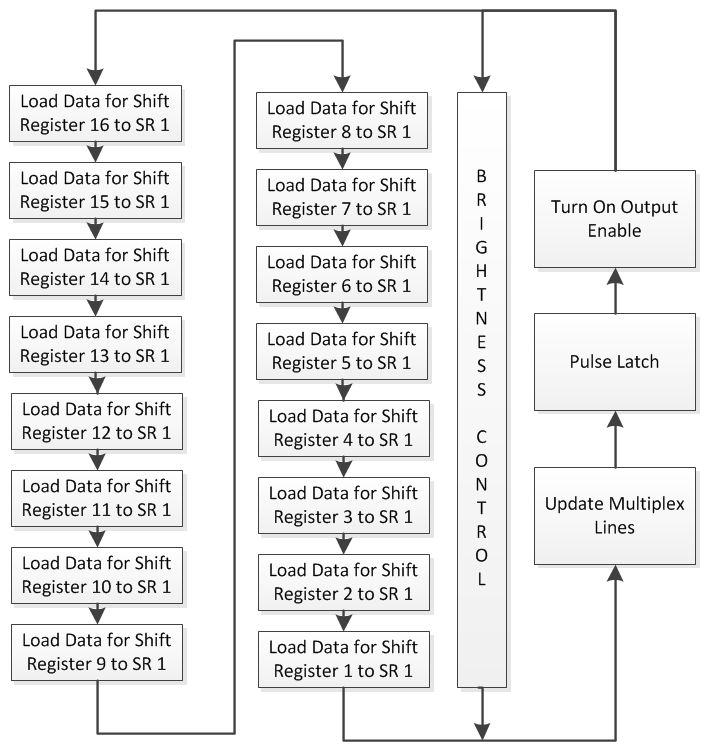
This sequence is also shown graphically below: